Internship in VLSI Design
Overview
Introducing Internship Program on VLSI Design
Description
Cranes Varsity is excited to unveil its 4-week VLSI Design Internship Program, tailored for aspiring engineers seeking hands-on experience in the field of VLSI.
The VLSI Design Internship Program spans four weeks, providing participants with comprehensive knowledge and practical skills in digital circuitry, VLSI design, digital logic, circuit design, and verification methodologies. Through a blend of theoretical sessions, lab exercises, and real-world projects, interns will develop a strong foundation in VLSI technologies. Under the guidance of experienced mentors, interns will work on cutting-edge VLSI projects, gaining expertise in areas such as RTL coding using verilog, synthesis, FPGA design, and verification using System Verilog. This practical experience will enhance their problem-solving abilities, critical thinking, and teamwork skills.
Cranes Varsity believes in a holistic learning approach, and interns will have access to mentoring sessions, industry interactions, and workshops, enriching their overall experience and providing valuable insights into the industry trends and best practices.
The VLSI Design Internship Program is open to students pursuing engineering in electronics, electrical, or related disciplines. A basic understanding of digital logic and familiarity with hardware description languages like Verilog or VHDL will be advantageous.
By participating in this 4-week internship, students will gain a competitive edge in the VLSI job market, equipped with both theoretical knowledge and practical experience. Cranes Varsity has a strong reputation for producing industry-ready professionals, further reinforcing the value of this program. Cranes Varsity has a proven track record of producing industry-ready professionals, further reinforcing the value of this program.
VLSI Internship Program ensures that a fresher is prepared on the entire essential aspects of the VLSI front end domain, including training on VLSI flow, SOC design, verification concepts, digital design, Verilog, and System Verilog. The VLSI design course content is well structured and mapped with leading industry requirements and their standards.
Lack of fundamentals in Advanced Digital Design, Analog Design and Verilog based design and verification becomes a major deterrent for freshers in finding the right career opportunities. VLSI Design Course ensures that freshers are empowered with all the essential skill sets required for various jobs in the VLSI front end domain. The course is completely practical oriented, with each aspect of the course involving multiple hands-on projects.
Course Objectives
Benefits of this program
- Internship with AICTE Registered company
- Concept to Project experience
- Exposure to real time scenarios and challenges
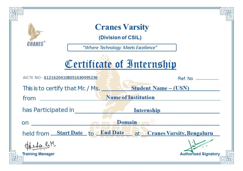
- Certificate of Participation
- Have strong fundamentals in HDL
- Gain exposure to industry standard FPGA Implementation
- Understanding Different Coding Methodologies
- To gain an Understanding of RTL coding for synthesis
- Write Verilog test fixtures for simulation
Tools and Resources
- Lattice Diamond Tool
Course Content (Syllabus)
Day1:
Brush Up on Digital Electronics
- Combinational
- Sequential Circuits
- Design of basic gates using mux
Day2:
Brush Up on Digital Electronics
- Counter design
- Design of digital circuits for given concepts
Day3:
Introduction to VLSI
- Design Flow of IC
- HDL
- Basic concept of Verilog
- Design Block
- Stimulus block
Day4:
Levels of Modeling
- Switch Level
- Gate Level
Day5:
Levels of Modeling
- Data flow
- Behavioral
Day6:
Implementation of Circuit using Verilog
- Combinational Circuits(Switch Level, Gate Level, Data flow, Behavioral level modeling)
- Sequential Circuits (Gate Level, Data flow, Behavioral level modeling)
Day7:
Design of Test Bench
- Introduction To TestBench
- Implementation of test benches for combinational circuits
- Implementation of test benches for sequential circuits
Day8:
Implementation of Counter using Verilog
- Up Counter
- Down counter
- Updown counter
Day9:
Implementation of Counter using Verilog
- Johnson counter
- Ring counter
- Excess 3 counter
Day10:
Implementation of Shift register using Verilog
- SISO
- SIPO
- PISO
- PIPO
Day11:
Implementation of Shift register using Verilog
- Arithmetic Shift operator usage for shift operation in Verilog HDL
Day12:
Implementation of Circuit using Verilog
- ALU
- MAC unit
Day13:
Design of FSM using Verilog
- Mealy Machine
Day14:
Design of FSM using Verilog
- Moore Machine
Day15:
Memory Modeling
- Design of Memory using RTL coding
- RAM Design(single and dual port)
- ROM Design
Day16:
Timer
- Introduction to Timer
- Implementation of timer using Verilog HDL
Day17:
PWM
- Introduction to PWM
- Implementation of PWM using Verilog HDL
Day18:
Frequency divider
- Introduction frequency divider
- Implementation of frequency divider using Verilog HDL
Day19:
Design of FIFO
- Introduction to FIFO
- Implementation of FIFO using Verilog HDL
MiniProject:
DesignofProtocols:
UART
- IntroductiontoUART
- Baudratecalculation
- AdvantagesanddisadvantagesofUART
- DesignofUARTusingVerilogHDL
SPI
- IntroductiontoSPI
- Advantagesanddisadvantages ofUART
- DesignofSPIusingVerilogHDL
Projects
Design of Protocols:
UART
- Introduction to UART
- Baud rate calculation
- Advantages and disadvantages of UART
- Design of UART using Verilog HDL
SPI
- Introduction to SPI
- Advantages and disadvantages of UART
- Design of SPI using Verilog HDL
Hiring Partners




















FAQs
Are you providing certification for this course?
Yes, we are providing Globally accepted certification for our courses with a grading system based on student performance
Is cranes Varsity training available online?
Yes, Cranes Varsity training is available through online
How does online training work?
Our Online training is Instructor-Led live online sessions
Do you provide training course material?
Yes, we will provide training course material for each module
Do you offer weekend classes?
Yes, we offer weekend classes as well evening classes.
Testimonials
First of all, I would like to extend my thanks to each and every member of Cranes Varsity. We were taught from the very basics of Embedded Systems Design which made it easier for students from all levels. I would like to extend my vote of thanks to cranes varsity to provide me with numerous opportunities.
Cranes are one of the top embedded training institutes in Bangalore. It has been a wonderful learning experience in Cranes Varsity. The training in every module of embedded systems at Cranes was effective. It provides a good platform for embedded systems. Cranes helped me get a job in the embedded industry.
It was a great experience in Cranes. My dream was to get into the embedded domain. As a fresher, it is difficult to get into the Embedded Design field, but Cranes made a huge difference in my career by giving the best training and placement assistance provided by Cranes. I would like to say Cranes is the best to choose for those who dream of embedded opportunity.
I take this opportunity to thank “CRANES VARSITY”, one of the best-embedded training institutes which are helping students to get into the best company to build their career. I thank all the trainers who enhanced my knowledge in every subject and the placement team for giving me the best opportunities in the field of embedded. Thank you for all your support.
Cranes varsity is the best Embedded Training Institute to learn both practical and theoretical knowledge. It is the best place to gear up your career in a core embedded industry. Management and faculty member support till you get placed. They provided lots of opportunities to me. The embedded Course modules that we learnt here are systematic, and I immensely earned great knowledge.
I am happy for Cranes for giving a platform and providing opportunities for attending the interview. Modules test, Mock test really helps to clear any company written test/ interview. Trainers were excellent at explaining and clarifying the doubts. I am very thankful to Cranes Varsity.
Cranes varsity is the best platform to improve your technical skills in Embedded System Design. Their dedication towards teaching modules and interaction with the students is commendable, which made me achieve good skills for my career growth in the electronics/semiconductor industry.
Happy to say that I am placed in Lekha Wireless. Cranes are one of the best Embedded Training Institutes. The way of teaching in Cranes is good. I thank the management and faculty for the guidance and opportunity.
If not Cranes, I would have been doing a job of not my interest and passion. Cranes provided me with the platform to start my career and knowledge about corporate life and requirements. “Thank you, Cranes” would be an understatement.

Ankita Saigal
Placed in Robert Bosch

Santhosh SM
Placed in L&T Technology

Mayur MN
Placed in L&T Technology

Chandru V
Placed in Avin Systems

Hemanth Kumar
Placed in Caravel Info Systems

Ankit Ahalawat
Placed in AK Aerotek Software

Nithin G
Placed in Moschip Semiconductor

Amitha Pankaj
Placed in Lekha Wireless

Sidharth S
Placed in L&T Technology

