PG Diploma in VLSI Design & ASIC Verification
( A Placement Oriented Program )
Design Intelligent Chips. Verify with Precision. Shape the Future of Semiconductors
100 % Placement Opportunities with
| Hands-On Projects Industry | Recognised Certification
Eligibility: BE, B.Tech, ME, M.Tech in ECE, EEE, E&I
(Graduate/Under Graduate /Working Professional)
One program, the complete silicon flow — design, verification and signoff
Most VLSI programs split RTL or verification into a single verification language. This one covers you from Verilog through SystemVerilog and UVM-based verification, then into EDA scripting, synthesis, STA, timing analysis and RTL-to-GDS physical design.
Design depth
Verilog RTL, synthesizable FSMs, timing-aware design and practical digital logic.
Verification mastery
SystemVerilog, UVM environments, coverage, assertions and reusable testbenches.
Silicon signoff
Synthesis, STA, timing constraints, STA reports, signoff checks and physical-design concepts.
Protocol-to-backend
Core controllers to bus logic to RTL-to-GDS concepts.
ASIC-grade verification
SystemVerilog, UVM and practical verification as practiced by verification teams.
Automation built in
Python and Tcl scripting for EDA tools, reports and repetitive work.
Timing closure skills
Constraints, setup/hold, clock paths, slack and timing reports.
Real FPGA hardware
Arty-7 FPGA and Zynq SoC boards for design implementation.
Industry and signoff tools
Vivado, QuestaSim, synthesis concepts and industry-style EDA workflows.
500 hours · 6 tracks · 13 modules · 2 capstones
Hardware Foundations → Core Programming → VLSI Design → Design & Verification → Scripting & Automation → Digital Physical Design & Timing Analysis
Electronics & Hardware Familiarization
The hardware fundamentals behind every chip
Core Electronics: Analog Circuits to Digital Logic Design
Reason about circuits, CMOS logic and the way digital systems are built.
Key topics
- Basic laws, RC circuits and power-supply basics.
- Diodes, rectifiers, Zener and clamping circuits.
- BJT and MOSFET switching, amplification and CMOS.
- Op-amps, filters and oscillators.
- Number systems and Boolean algebra.
- Logic gates, multiplexers, encoders and decoders.
- Flip-flops, counters and shift registers.
- Finite state machines and timing fundamentals.
Core Programming
C and object-oriented C++
Mastering C Programming (Self-Study)
Build core programming skills through guided self-study.
Key topics
- Basic C program structure.
- Variables, operators and data types.
- Decision statements and loops.
- Arrays and strings.
- Sorting and searching.
- Functions and pointers.
Mastering OOP using C++
Learn the object-oriented concepts used later in SystemVerilog and UVM.
Key topics
- OOP concepts: class, object and namespace.
- Classes, objects, abstraction and encapsulation.
- Access specifiers and the this pointer.
- Constructors and destructors.
- Inheritance and polymorphism.
- Operator overloading, templates and STL.
- Problem-solving practice.
VLSI Design
RTL, protocols and FPGA
RTL Coding with Verilog
Build synthesizable RTL for combinational and sequential digital designs.
Key topics
- HDL fundamentals, design methodology and data types.
- Gate-level, dataflow and behavioral modeling.
- Procedural blocks, operators and delays.
- Combinational and sequential circuits.
- Blocking and non-blocking assignments.
- if/else, case, loops and generate statements.
- Functions, tasks, counters and FSMs.
- Testbench fundamentals and simulation.
On-Chip Protocols Design
Design and simulate common serial and SoC bus protocols.
Key topics
- Serial communication protocols.
- UART.
- I²C.
- SPI.
- AMBA architecture.
- AXI4.
FPGA Programming
Implement, debug and demonstrate digital designs on FPGA hardware.
Key topics
- FPGA architecture: CLBs, IO blocks and interconnects.
- FPGA design flow and tools.
- Up, down and up-down counters.
- Shift registers and Mealy/Moore FSMs.
- Debugging with VIO and ILA.
- Project demonstration on FPGA.
Capstone: RTL-to-hardware digital design implementation.
Design & Verification
SystemVerilog, UVM and protocol-level testing
Design and Verification using SystemVerilog
Build class-based verification environments with coverage and assertions.
Key topics
- Data types, enums, structs and unions.
- Dynamic, packed, unpacked and associative arrays.
- Processes, fork-join and synchronization.
- Classes, inheritance, polymorphism and encapsulation.
- Deep and shallow copy; static and virtual classes.
- Functional and cross coverage.
- Assertions and verification planning.
- Complete verification environment.
ASIC Verification using UVM
Develop reusable UVM components and scalable testbench environments.
Key topics
- UVM base classes and factory concepts.
- UVM phases, objections and configuration database.
- Sequences, sequencers and drivers.
- Monitors, agents and scoreboards.
- TLM ports and analysis communication.
- Reusable testbenches and regression concepts.
On-Chip Protocol Verification
Verify a protocol design using structured SystemVerilog/UVM testbenches.
Key topics
- Protocol test planning and stimulus.
- Directed and constrained-random tests.
- Monitor, scoreboard and checking.
- Functional coverage and assertions.
- Regression, debug and coverage closure.
Capstone: Protocol verification using a reusable testbench.
Scripting & Automation
Python and Tcl for EDA flows
Python Scripting
Automate repeatable tasks, reports and engineering workflows with Python.
Key topics
- Python fundamentals and functions.
- File handling and parsing text reports.
- Lists, dictionaries and data processing.
- Automating repetitive EDA tasks.
- Log extraction and report generation.
- Workflow utilities and scripting best practices.
TCL Scripting
Use Tcl to automate common EDA tool commands and flow steps.
Key topics
- Tcl syntax, variables and expressions.
- Lists, loops, conditionals and procedures.
- Reading and writing files.
- Automating tool commands and flow steps.
- Running scripts and extracting reports.
- Basic flow control and debugging.
Digital Physical Design & Timing Analysis
Synthesis, STA and RTL-to-GDS concepts
Digital Physical Design
Understand the digital implementation flow from RTL and synthesis toward physical design.
Key topics
- RTL-to-gate synthesis flow and netlists.
- Synthesis constraints and optimization concepts.
- Floorplanning, power planning and placement.
- Clock-tree synthesis and routing concepts.
- Physical verification and design-rule checks.
- Area, power and performance trade-offs.
- Flow stages and implementation reports.
Static Timing Analysis
Analyze timing paths and understand timing constraints and closure.
Key topics
- STA fundamentals and timing paths.
- Setup and hold checks, slack and timing reports.
- Clock definitions and uncertainty.
- Input/output delays and timing constraints.
- Clock skew, latency and clock relationships.
- Critical-path analysis and timing optimization.
- Timing exceptions and constraint basics.
- Introduction to signoff timing workflows.
Tools, platforms & hardware
Capabilities you’ll graduate with
Practical engineering skills across RTL design, verification, automation and silicon implementation, backed by hands-on work.
Think like a designer — CMOS, logic, FSMs and timing fundamentals.
Write production RTL — clean, synthesizable Verilog for datapaths and controllers.
Design SoC interfaces — UART, SPI, I²C and AXI4 controllers.
Run on FPGA — implement, debug and validate RTL on real hardware.
Verify with SystemVerilog — classes, coverage and assertions.
Construct UVM testbenches — reusable components, sequences and scoreboards.
Automate EDA flows — Python and Tcl for scripts, logs and reports.
Close timing — understand constraints, reports, slack and STA concepts.
Think RTL-to-GDS — synthesis, physical implementation and signoff flow concepts.
Projects you’ll ship
| Project | Skills developed |
|---|---|
| UART, SPI, I²C and AXI4 Controller Design | RTL design, protocol logic, simulation |
| FPGA Design & Debugging | FPGA implementation, VIO/ILA debug |
| SystemVerilog Verification | Classes, assertions, functional coverage |
| UVM Protocol Verification | Reusable testbench and regression concepts |
| Python/Tcl EDA Automation | Scripts, report parsing and workflow automation |
| Digital Physical Design & Timing Analysis | Synthesis, constraints, STA and signoff concepts |
Project selection and depth may depend on the course delivery plan and learner progress.
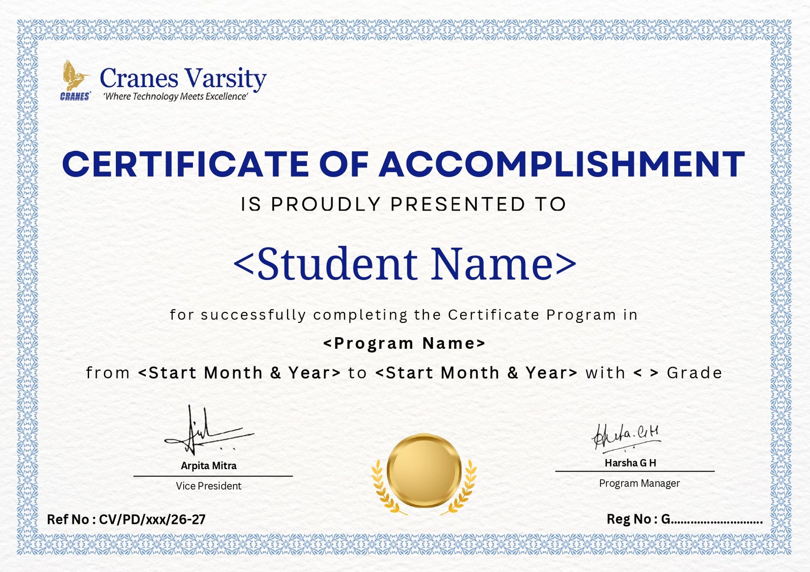
Three certifications, one progression
RTL Design Certification
Verilog fundamentals, synthesizable RTL and digital design projects.
Verification Certification
SystemVerilog, UVM and practical verification skills.
ASIC Physical Design & Signoff
EDA scripting, timing analysis and physical-design flow concepts.
Assessments and project reviews help learners demonstrate practical skills across the program.
Built for RTL, verification and silicon careers
Industry-focused skills and placement assistance for semiconductor roles, powered by career-focused learning.
Learn
Structured modules, technical resources and self-paced practice.
Practice
RTL labs, verification exercises, FPGA boards and guided projects.
Assess
Domain assessments, skill-gap analysis and screening-test preparation.
Get placement-ready
Interview preparation, resume and project readiness, and job-search support.
Industry job roles
Industries hiring
Semiconductor and chip design, ASIC and SoC design services, FPGA-based product development, EDA and verification services, automotive and consumer electronics.
Who should enroll?
ECE/EEE and related graduates, CSE students with interest in digital hardware, and fresh graduates aiming for VLSI careers.
Early-career engineers seeking to build skills in RTL design, verification, scripting or timing analysis.
Hiring Client
Frequently asked questions
What is the duration of the PG Diploma in VLSI Design & ASIC Verification?
The program runs for a total of 500 hours at 4 hours per day, delivered offline and instructor-led.
How is this PG Diploma different from a diploma in VLSI?
Beyond Verilog RTL, FPGA, SystemVerilog and UVM, it adds on-chip protocol verification, Python and TCL scripting for EDA automation, static timing analysis and digital physical design from RTL to GDS-II.
What does the physical design and timing track cover?
Synthesis, constraints, static timing analysis, PVT corners and OCV, floorplanning, placement, clock tree synthesis, routing, DRC, LVS, IR drop, EM and GDS-II generation, with exposure to Cadence Innovus and Synopsys IC Compiler II flows.
Which tools and boards will I use?
Learners work with Xilinx Vivado, QuestaSim, EDA Playground, Yosys and OpenTimer, on Artix-7 FPGA and Zynq SoC boards.
How many certifications and capstones are included?
The program includes 3 certifications and 2 capstone projects: RTL to Realization on FPGA, and Functional Verification from SystemVerilog to UVM.
What jobs can I apply for after the program?
Roles include RTL Design & Verification Engineer, FPGA Design & Development Engineer, Design & Verification Engineer, ASIC/SoC Verification Engineer, Functional Verification Engineer and Silicon Validation Engineer.