Advanced Diploma in VLSI Design & Verification
( A Placement Oriented Program )
Design the Future. Engineer the Next Generation of Semiconductors.
100 % Placement Opportunities with
| Hands-On Projects Industry | Recognised Certification
Eligibility: BE, B.Tech, ME, M.Tech in ECE, EEE, E&I
(Graduate/Under Graduate /Working Professional)
Why choose this VLSI design & verification program?
Build job-ready skills for the semiconductor industry — core electronics, Verilog RTL, on-chip protocols, FPGA implementation and verification with SystemVerilog and UVM, backed by C++ and Linux fundamentals.
Complete front-end flow
Design → simulate → implement on FPGA → verify.
Industry verification skills
SystemVerilog and UVM, the core verification tools used by verification teams.
Hands-on FPGA hardware
Arty-7 FPGA and Zynq SoC boards with VIO and ILA debugging.
Industry-standard EDA tools
Vivado, QuestaSim and EDA Playground.
Protocol design expertise
UART, SPI, I²C and AMBA AXI-4.
Flexible learning mode
Online or offline training with hands-on digital academy learning.
Project-based learning
An RTL-to-verification project plus capstone projects.
VLSI curriculum: 4 phases, 9 modules
Hardware Foundations → Programming Fundamentals → VLSI Design → VLSI Specialization
Electronics & Hardware Familiarization
The electronics behind every chip
Core Electronics: Analog Circuits to Digital Logic Design
Understand analog and digital electronics — from transistors and CMOS to FSMs and timing.
Key topics
- Ohm’s law, RC circuits and power-supply basics.
- Diodes, rectifiers, Zener and clamping circuits.
- BJT and MOSFET switching, amplification and CMOS.
- Op-amps, filters and oscillators.
- Number systems and Boolean algebra.
- Logic gates, multiplexers, encoders and decoders.
- Flip-flops, counters and shift registers.
- Finite state machines.
- Basics of timing analysis.
Core Programming Fundamentals
C, C++ and Linux
Mastering C Programming (Self-Learning)
Build core C programming skills through self-paced learning.
Key topics
- Simple C program structure.
- Variables, operators, decision statements.
- Arrays.
- Sorting and searching.
- Strings.
Mastering OOP using C++ & Competitive Problem Solving
Write object-oriented C++ — the foundation for SystemVerilog classes and UVM testbenches.
Key topics
- OOP concepts: class, object and namespaces.
- Classes, objects, abstraction and encapsulation.
- Access specifiers and the this pointer.
- Constructors and destructors.
- Friend and operator overloading.
- Inheritance and runtime polymorphism.
- Exception handling, templates and smart pointers.
- Templates and STL.
- Problem solving using HackerRank.
Linux System Programming using C
Linux in action
VLSI Design
RTL, protocols and FPGA
RTL Coding with Verilog
Write synthesizable Verilog for combinational and sequential logic, FSMs and testbench basics.
Key topics
- HDL fundamentals, design methodology, data types and operators.
- Gate-level modeling, procedural blocks and delays.
- Dataflow modeling, continuous assignments and operators.
- Combinational and sequential logic.
- Behavioral modeling: always blocks, blocking vs non-blocking assignments.
- if-else, case, loops, generate, wire, reg, forever and repeat.
- Sequential and parallel blocks, fork-release and de-assign.
- Functions, tasks and testbenches.
- FSMs, counters and shift registers.
- Functions, tasks and generate statements.
- Verify and ModelSim/Questa simulation basics.
On-Chip Protocols Design
Design and simulate the serial and on-chip bus protocols used in SoC design.
Key topics
- Basic communication protocols.
- UART.
- I²C.
- SPI.
- AMBA architecture.
- AXI4.
FPGA Programming
Implement, debug and demonstrate digital designs on FPGA hardware.
Key topics
- FPGA architecture: CLB, IO blocks, interconnects.
- CPU vs FPGA: design flow and tools.
- Configurable logic and LUTs on FPGA.
- Up, down, up-down, Johnson and ring counters.
- Shift registers and Mealy/Moore FSMs.
- Debugging with VIO and ILA.
- Project demonstration on FPGA.
VLSI Specialization — Verification
SystemVerilog and UVM
Design and Verification using SystemVerilog
Build class-based verification environments with coverage and assertions.
Key topics
- Need for SystemVerilog; verification environment.
- 2-state, 4-state, enum, string, struct, union and class types.
- Dynamic, packed, unpacked and associative arrays.
- fork-join, join_any, join_none and wait fork.
- OOP: inheritance, polymorphism, data hiding, encapsulation.
- Deep and shallow copy; static and virtual classes.
- Functional and cross coverage.
- Assertions with examples.
- Building a complete verification environment.
Verification using UVM
Build reusable, industry-standard UVM testbenches.
Key topics
- Why UVM; UVM objects and base classes.
- UVM macros and data-type methods.
- UVM phases, config DB and objections.
- TLM ports, analysis ports, FIFOs and sockets.
- UVM callbacks.
- UVM testbench components and reusable testbench.
Tools, software & hardware
What you’ll be able to do
Master digital fundamentals — CMOS, logic design, FSMs and timing basics.
Program in C and C++ — for OOP and competitive problem-solving for verification work.
Write RTL in Verilog — synthesizable combinational, sequential and FSM designs.
Design on-chip protocols — UART, SPI, I²C and AMBA controllers.
Implement on FPGA — synthesis, program and debug with VIO and ILA.
Verify with SystemVerilog — classes-based testbenches, coverage and assertions.
Build UVM testbenches — reusable, industry-standard verification environments.
Ship complete projects — from RTL to FPGA realization and full verification.
Hands-on & capstone projects
| Project | Skills developed |
|---|---|
| Multi-Client Chat App, Memory Leak Detection Toolkit & Commerce Cart Simulator | C++, OOP, problem solving |
| Concurrent Chat Server using Socket Programming | Linux, networking, concurrency |
| UART, SPI, I²C & AXI4 Controller Design | RTL design, protocol design, simulation |
| Digital Controllers & ALU Cores on FPGA | Design, simulation, FPGA implementation and verification |
| SystemVerilog Verification of Controllers, CPU Cores & Protocols | SV testbenches, coverage, assertions |
Project selection depends on learner readiness, project scope and curriculum coverage.
Certification path
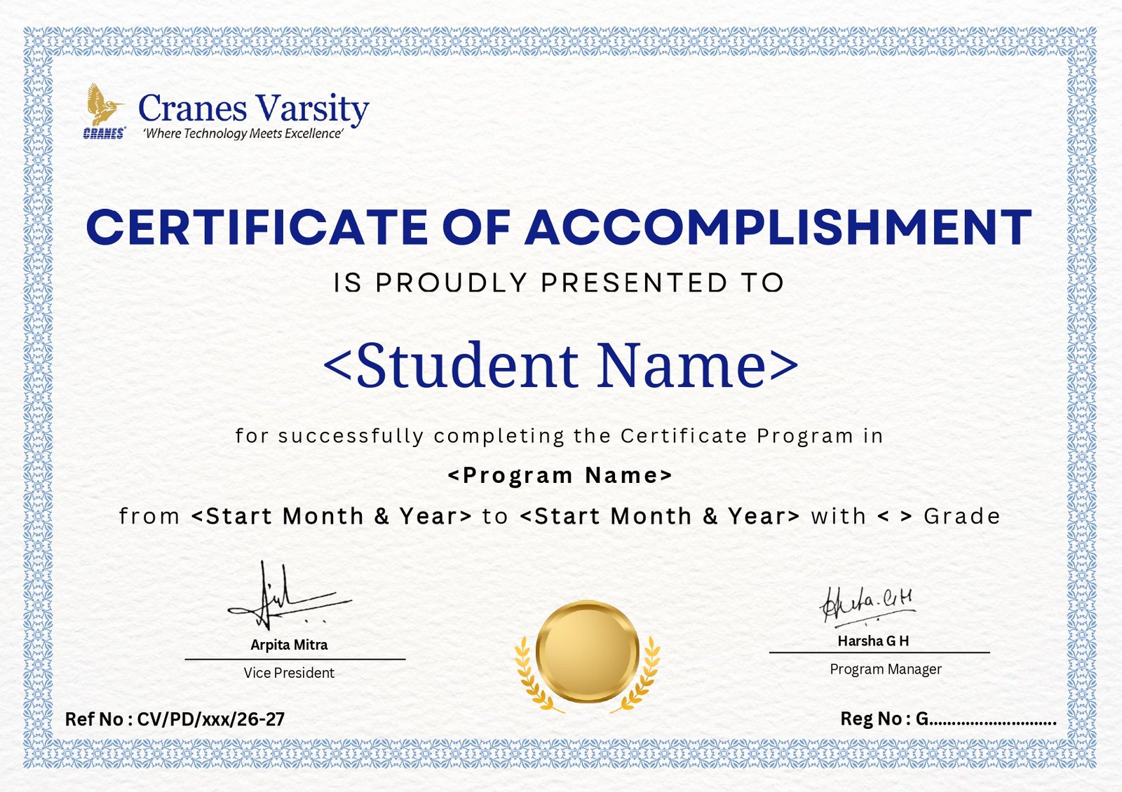
[Certification name]
Awarded after all modules, assessments and capstone projects.
Assessment through module assignments, hands-on labs, FPGA demonstrations and capstone project reviews.
VLSI jobs: from classroom to career
Interview readiness and placement assistance, powered by career-focused learning.
Learn
Structured modules, technical resources and self-paced sessions.
Practice
Hands-on labs on Verilog, QuestaSim and FPGA boards, plus guided practice.
Assess
Domain assessments, skill-gap analysis and screening-test preparation.
Get placement-ready
Interview prep, portfolio guidance, resume and project readiness, and job opportunities.
Industry job roles
Industries hiring
Semiconductor and chip design, ASIC and SoC design services, FPGA-based product development, EDA and verification services, automotive and consumer electronics.
Who should enroll?
ECE/EEE students and graduates, CSE, ECE, EE and related branches.
Fresh graduates aiming for VLSI design and verification careers.
Early-career engineers seeking to upskill in RTL design or verification.
Hiring Client
Frequently asked questions
What is the duration of the Diploma in VLSI Design & Verification?
The program runs for a total of 300 hours.
Is the VLSI course online or offline?
The program is available online and offline, supported by the Cranes Digital Academy platform.
Which tools and boards will I use?
Learners work with Xilinx Vivado, QuestaSim and EDA Playground, on Artix-7 FPGA and Zynq SoC boards.
Does the program cover verification?
Yes. The specialization covers Design and Verification using SystemVerilog and Verification using UVM.
What projects will I build?
Projects include protocol controllers (UART, SPI, I2C, AXI4), digital controllers and ALU cores on FPGA, SystemVerilog verification of controllers and CPU cores, and C++ and Linux applications.
What jobs can I apply for after the course?
Roles include VLSI Design Engineer, RTL Design Engineer, FPGA Engineer, ASIC Design Engineer, Verification Engineer and Graduate Engineer Trainee.